

Discover more from Mr Market Miscalculates
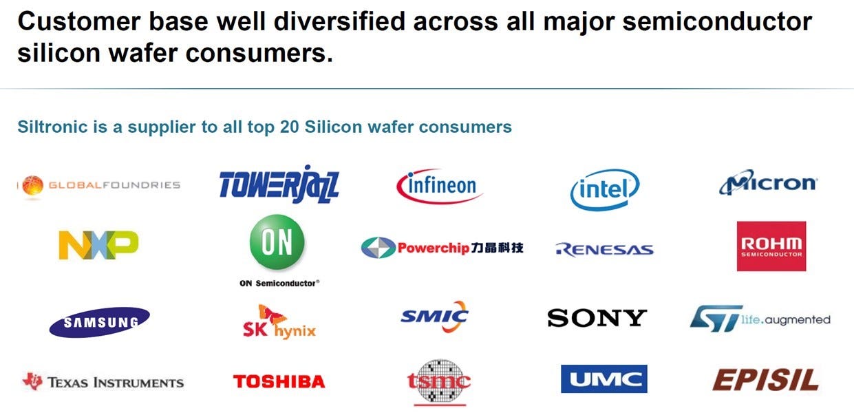
Headquartered in Munich and with four production facilities (2 in Germany - Freiberg and Burghausen -, one in the US – Portland - and one in Singapore), Siltronic AG (WAF GR) is the fourth-largest producer of silicon wafers, supplying all top 20 silicon wafers consumers.
While the company exists in its current form since 2004, its original concept goes back to 1953 with the initial research in the high-purity silicon area and the development of the first silicon wafer in 1962. In 1968 the business was incorporated as Wacker-Chemitronic and changed name to Wacker Siltronic in 1994. In 2000, it set up a joint venture with NSC Electron (part of Nippon Steel) and made this a wholly owned subsidiary in 2003. The company listed as a stand-alone entity in 2015.
Wacker Chemie has been selling down its stake since the IPO and today owns ~31% of the shares, with GlobalWafers (a Taiwanese company) owning around 14% and the rest being free-float.
An abridged primer on silicon wafers
Silicon wafers are thin discs made of silicon that are used to make semiconductors and are the largest segment of the semiconductor material market. In addition, silicon wafers are also used for photoelectric (solar) cells.
The entire production of chips can be divided into front-end processes (involving circuit formation) and back-end processes (involving cutting, packaging, and shipping chips formed from these circuits).
The term semiconductor is a catch-all name for substances that can either conduct electricity well or act as an insulator depending on conditions. Only a few substances can act as semiconductors, including silicon, germanium and gallium. Amongst these, silicon wafers are used as the raw material for just about all semiconductors because of their many advantages: they are cheap (silicon is the second most abundant element after oxygen), easily processed, and can readily be scaled up.
Silicon wafers are produced by heating a mixture of silica and carbon in a furnace, creating wafer-grade silicon. A seed is then dipped into the molten silicon and is slowly twisted and pulled out. This creates a cylindrical ingot several feet long, which is ground to an appropriate diameter. The ingot is then sliced into thin wafers for shipment to Integrated Device Manufacturers (IDMs) and foundries.
Reducing semiconductor process costs entails two approaches: increasing wafer diameter or miniaturisation of semiconductor wiring. Larger-diameter silicon wafers have contributed to the reduction in production costs as more chips can be made from one wafer: the area of a 300mm wafer is 2.25x larger than the area of a 200mm wafer.
The evolution of silicon wafers is largely a history of expanding disc diameter: wafers were 100mm (4inch) in diameter in 1975, 150mm (6inch) in 1980, 200mm (8icnh) in 1991, and 300mm (12inch) wafers were introduced in 2001. The latter are today the mainstream size in particular for advanced chips - such as processors, SoC and memory - but 200mm wafers still have a significant share. While possible, most companies are not yet positive on a move to 450mm wafers.
Growth in the number of manufacturers (latter half of 1980s). Traditionally dominated by the large Japanese keiretsu, more business diversification by these conglomerates led to the entry of new participants in 1987, such as Nippon Steel’s subsidiary Nittetsu Denshi and Showa Denko Silicon. This was followed by more entrants such as Monsanto Electronic Materials Company (MEMC)’s construction of a factory in Japan and the number of silicon wafer manufacturers at this time is believed to have been over fifteen.
Number of manufacturers consolidates (1990s to first half of 2000s). From 1990 to 2000, the industry witnessed consolidation and a reduction in the number of manufacturers through the sale of businesses and by reorganisation and integration. This consolidation was the result of the massive increase in capital expenditure and R&D expense that accompanied the increase in wafer diameters, and attrition caused by lower earnings due to excessive competition in the era of small diameter wafers. In 1998, Showa Denko pulled out of the business and Nippon Steel established a joint venture between its subsidiary NSC Electron and Wacker under the name Wacker NSCE. Subsidiaries of Sumitomo and Mitsubishi created in 2002 the joint-venture Sumitomo Mitsubishi Silicon (which changed name to SUMCO in 2005) and subsequently purchased Komatsu Electronics Metals, thereby reducing the number of 300mm-wafer manufacturers to six.
Revival of investment in silicon wafers (latter half of 2000s). Semiconductor manufacturers withdrew from silicon wafers. Sino-American Silicon’s (SAS) purchase of the Covalent Materials’ silicon wafer business brought that company into the SAS fold but the former name of Covalent Materials was Toshiba Ceramics, the silicon wafer company in the Toshiba group. Hitachi, at one point, also had a silicon wafer business, which was sold to Shin-Etsu Chemical in 1999. This trend started to change around 2006. Silicon wafer shortages started to appear (the rapid growth in solar cells left polysilicon in short supply) and some semiconductor companies were hit by high wafer prices, which led to their increased involvement in the wafer business through joint ventures and other measures. Samsung Electronics established a 300mm-wafer production capacity through a joint venture with Wacker Chemie/Siltronic.
Weak profitability (2008-2016). In the late-2000s, aggressive investment resulted in excess capacity and wafer prices declined, leading to a reduction in earnings. Companies overestimated 300mm wafer demand for DRAMs, NAND Flash memories and other applications, and all of them aggressively increased capacity. However, demand growth slowed, particularly for DRAMs, in line with the shift in demand from PCs to smartphones. Semiconductor demand fell in the early 2010’s owing to a reduction in the number of semiconductors per device. As a result, slow growth in silicon wafer demand and reduction in prices stemming from excess capacity put substantial pressure on earnings at the silicon wafer companies.
All the major companies were forced to embark on personnel cuts and facility closures: most of the makers concentrated on reducing capacity for smaller diameter wafers. The result was another restructuring in the industry. Taiwan’s GlobalWafers (which originated as a spin-off from Sino American Silicon) acquired the silicon wafer business of Covalent Materials in 2012, and Topsil and SunEdison Semiconductor (previously MEMC, the last major US-based silicon wafer maker) in 2016, which enabled it to become the world’s third largest player. Parent companies also made several divestitures. Siltronic itself was listed through an IPO, with Wacker Chemie later carrying out additional share sell-offs and reducing its holding. Nippon Steel & Sumitomo Metal and Mitsubishi Materials, which were major shareholders in SUMCO, also gradually sold off their stakes, from around 28% each to 13% each by 2017.
Earnings recovery and resumption of capex (2017 onward). While the focus of capacity increase shifted to small-scale measures such as debottlenecking, there was an increase in NAND Flash demand for data centres and an increase in the number of semiconductors used in electronic devices with the move to higher performance smartphones. These favourable conditions sparked a recovery in growth potential for semiconductor demand. As a result, the supply/demand balance for silicon wafers started getting tighter and there were signs of a price recovery. By 2017 there was a resumption of interest by semiconductor companies in holding wafer makers, with SK Group (which includes SK Hynix) taking a majority stake in SK Siltron (previously LG Siltron).
Siltronic’s products and markets
Hyper-pure silicon wafers are the basis for almost all semiconductor devices and consequently represent an essential basis for the world’s electronics industry. Many electronic devices would be inconceivable without the shiny gray-black metalloid silicon: smartphones, televisions, cars, wind turbines, …
Currently, WAF manufactures and sells hyper-pure semiconductor silicon wafers with diameters of up to 300mm: it also offers polished wafers (extremely flat and with a mirror-like surface, they satisfy the highest standards in terms of flatness and surface quality) and epitaxial wafers (based on polished wafers, epitaxial wafers feature an additionally deposited monocrystalline surface layer).
65% of the portfolio is made up of 300mm wafers, with the remaining 35% in 125mm-250mm and SD wafers. In terms of end customers, 72% of sales are to Asia, with Europe at 18% and US at 10%.
The global semiconductor industry sales totalled around US$550 billion in 2021, a record high and a 26% increase compared to 2020. The record sales growth was driven by a combination of strong demand linked to the rebound of the global economy, stockbuilding in response to a shortage across the semiconductor supply chain (particularly in the automotive industry), and price increases related to logistics costs and raw material prices. To strengthen the resilience of their semiconductor supplies, companies have increased their inventories, moving from a “just-in-time” policy to a “just-in-case” strategy.
Of this market, the silicon wafers segment represents around US$13 billion.
Global megatrends (5G, artificial intelligence, connected objects and electric vehicles) drive sustained increase in wafer area: devices become increasingly intelligent and require continuous improvement in functionality and energy efficiency.
Demand for mobile data, driven mainly by video, is growing 30% every year and shows no signs of slowing down. Mobile communication – particularly smartphone-based – is expanding and will continue to expand beyond what is possible today, offering new – and ever more secure – services from health to self-driving vehicles and smart homes. Beyond performance alone, the challenge is to make mobile communication more environmentally friendly and inclusive, as well as to connect the unconnected.
The car of tomorrow will have multimedia content and be fully autonomous, safer and greener. These trends will shape the future of mobility with a focus on passenger comfort, convenience, safety and reducing the carbon footprint. The automotive electronics segment is part of the fastest growing market in the semiconductor industry.
Industry fundamentals
Silicon wafers have three main characteristics: they are market-based goods, have huge fixed costs, and have a major 6-7 years’ business cycle.
Silicon wafers are even more commoditised than chips are, and are particularly sensitive to supply and demand factors. Although there is a certain level of quality improvement and product differentiation in response to customer demand, there are no major technical differences between the top manufacturers.
Still, they incur high capex and carry an onerous fixed cost burden. Even if capacity shortages arise, it does not lead directly to active capital expenditure, and prices tend to rise. On the other hand, there is a considerable incentive for companies to maintain operating rates even when surplus capacity emerges, and prices easily fall.
This is a business with high barriers to entry and limited competition among major manufacturers. Five/six companies compete in the 300mm wafer business, but this is not an easy market to enter, due to:
Most of the machinery used in production is developed in-house, and there are high technological barriers. Major firms purchase general equipment and then customise it: they buy some items such as testers and epitaxial wafer equipment, but make much of their grinding, polishing, and other equipment themselves. There are no companies providing the full range of silicon wafer equipment, while the market for such equipment is small-scale, limiting entry into this business. A high degree of specialisation also implies a high degree of human capital required: not every city or nation in the world can have access to the required pool of talent.
Customers demand high quality (flatness and cleanliness) for miniaturisation and reliability. Silicon wafers are sort of commodity products, but they are order-made for individual customers, particularly with state-of-the-art products. Miniaturisation demands high-quality wafers, while automotive semiconductor wafers need to be very reliable.
The consumer base is also concentrated: securing the first contract can be challenging
There is no benchmark price, such as a spot market price, and in most cases, prices are decided quarterly or semi-annually through bidding and negotiation. In Taiwan, prices are largely decided on a quarterly basis, usually by auction. In other regions, such as Korea and Japan, prices are typically decided on a half-year basis, usually by negotiation.
Demand is mostly linked to semiconductor volume. And within semiconductors, memory is a major driver of wafer demand, with the top five companies combining for an over 70% share.
The silicon wafers business is also highly consolidated on the supply side: it’s dominated by two Japanese firms, Shin-Etsu Handotai (with a 29% market share) and SUMCO (22%), followed by GlobalWafers (Taiwan, 15%), Siltronic (12%), SK Siltron (Korea, 11%) and France’s Soitec (6%). Several players from China also compete in the silicon wafer business.
The industry has been difficult to invest in as the massive expansion of capacity in the 90’s and 00’s (similar to fibre capacity) led to negative/feeble returns on capital. Due to this excessive capital cycle, capacity has largely remained unchanged over the past decade, for a simple reason: it is incredibly expensive.
The failed takeover
The silicon wafer business continues to consolidate amid booming demand and shortages in the market: the list of wafer manufacturers keeps getting shorter.
In December 2019, GlobalWafers, the world’s third-largest manufacturer, offered €120 for all outstanding shares of Siltronic, later raising the offer to €145 (for a total equity value of €4.4bn). That was a 50% premium to then recent prices, but still below the €160 that Siltronic shares traded at in 2018, when its operating margins peaked at 34% (the following year the margin fell to 26% and it was 16% in 2020). GlobalWafers wanted to strengthen its presence in Europe, where Siltronic is the leading supplier: the merged company would have jumped to the second position and a serious rival to Japan’s Shin-Etsu, the top manufacturer.
Already in 2015, just after the IPO, Siltronic’s CEO said:
“Consolidation is a very interesting subject. Everybody is talking about it and has been relatively outspoken about the idea and about who will participate and who will not participate and we will stick to it that consolidation without Siltronic participating is not very likely to happen. On the other hand, we continue to focus on things we can influence on our own, which is technology performance, quality performance, and cost cutting performance. So yes, it is a topic on our agenda but not the hottest topic.”
However, in February 2022 GlobalWafers’s offer expired as its conditions were not fulfilled within the applicable deadline: the German Federal Ministry for Economic Affairs and Climate Action did not issue a certificate of non-objection, thus killing the transaction despite Wacker-Chemie having already agreed to sell its 31% stake to GlobalWafers. Siltronic only got a €50 million termination fee. GlobalWafers is expected to sell its 14% stake (no buyers yet), which is also weighting the price down.
Berlin’s failure to clear the transaction highlights how national security concerns over supply chains are shaping deals in the semiconductor industry, and will slow down consolidation.
Financials and valuation
Siltronic has one of the strongest balance sheets in the industry: even after the recent €300 million ESG-linked bond emission and the €200 million drawdown in a European Investment Bank loan (both to fund current capex), the company is still expected to finish the year with at least €200 million in net cash & short-term investments.
On the standard metrics, Siltronic appears extremely cheap:
P/E (2022e): 7x
P/E (5Y trailing): 9x
EV/EBIT: 5x
FCF yield: 16%
Dividend yield: 3.8%
[Note: FCF yield is so high because of the huge change in prepayments in 2022; normalising this value FCF yield is around 5%]
It also trade at approximately 0.5x total capital invested, but as already noted the assets’ replacement value is much higher.
Siltronic has similar (if not better) returns than the largest competitors, and operating margins not much lower: still, it trades at a 30%-40% discount to their multiples.

This is despite WAF reiterating at the Q3 results announcement their targets for full year 2022 softness in some end markets leads to the risk of inventory corrections in some segments, but long-term growth drivers are intact and the structural shortage for 300mm wafers is expected to persist (fx tailwinds are also helping sales and profits). And contrary to several European manufacturers, Siltronic has not pre-announced any reduction in activity due to high energy prices: quite the opposite, the project of becoming independent of gas supply at its German sites is proceeding.
The two elephants in the room: capex and unfunded pension funds
For the first element, WAF is in the middle of refurbishing and making more efficient the 300mm factory in Singapore: construction is well on track, the first wafers should be out by 2024 and the total capex is expected to be around €2 billion.
For the second point, similar to many other German companies, over the last decade WAF has suffered from the burden of high unfunded pension plans, which reached a peak of almost €600 million in 2020 (WAF operates both defined contribution and defined benefit plans).
Over the past few months, with macro-economic conditions changing all over the world, the scenario has changed as higher interest rates are a big positive for companies that have large pension deficits.
This is indeed what WAF reported in 2021:
“On the one hand, pension liabilities have decreased, which is primarily due to rising interest rates: In the USA, the interest rate for pensions rose from 2.07 percent at the end of 2020 to 2.51 percent at the end of 2021, and in Germany from 0.69 percent to 1.23 percent in the same period.” (Siltronic 2021 annual report)
And even more in H1 2022:
“The overall economic development has recently also triggered a significant rise in interest rates. This results in a massive reduction in our pension provisions. Combined with the profit, this leads to an increase in our equity ratio from 53.7 percent on December 31, 2021, to 56.7 percent.”
“The reason for the decrease in pension obligations was the interest rate development in Germany and the USA. As of 30 June 2022, the pension provision in the USA was discounted at 4.16 per cent, com-pared to 2.51 per cent as of 31 December 2021. In Germany, the interest rate rose from 1.23 per cent to 3.3 per cent.” (Siltronic H1 2022 report)
From the pure accounting point of view, this is indeed “correct”: the present value of future liabilities is lower when discounted at higher interest rates. However, there are other factors which need to be taken into consideration: 1) when interest rates increase, asset values are also hit; 2) many pension plans are indexed either to salaries or inflation: if inflation goes up, future payments will also increase.
The pensions sensitivity analysis published by companies typically relate only to the liability side, not to the asset side; this is what WAF disclosed at the end of last year:
And the composition of the plans:
Interest rate sensitivity dominates everything else (a further 2% increase from end of last year would reduce future obligations by more than 35%!), but again, this doesn’t cover the effects on the asset side. In addition, the assumed pension increases (+1%/+1.8% p.a., image below) and the salary growth rates (+2.5% in Germany, +3% in the US) might both underestimate the impact of a more permanent inflation.
Risks
Customer concentration: Siltronic’s top customers include Infineon, Intel, Samsung, SK Hynix and TSMC (although it does disclose the level of concentration)
Bigger scale means lower fixed costs (as a % of a sales): because of scale, SUMCO and Shin-Etsu have historically generated higher margins and captured a disproportionate share of industry profits
Technology can change quickly and require huge investments to catch up: Siltronic spends on average 6% of sales on R&D
Perpetual pricing pressure: there have been long periods in the past of continuous price declines, when wafer makers tried to carry out price hikes, but related announcements came amid a worsening supply-and-demand balance and price hikes were not achieved
Rise of 5G, which requires more silicon-on-insulator (SOI) wafers: while this segment is still limited (Soitec has a 65%-70% market share, based on their own estimations), Siltronic is the only manufacturers in the top 5 not to produce them
Conclusions
The silicon wafer business typically flies under the radar, but it’s a fundamental part of the semiconductor business: every chipmaker needs to buy silicon wafers in one size or another.
That said, the business is capital intensive and volatile which leads to significant fluctuations in stock prices. And the products are pretty commoditised, which means there are little chances to truly differentiate yourself and being at the mercy of demand/supply forces.
So, this stock is probably better traded than held for the long-term.
The current price seems indeed interesting:
The business is not going to disappear overnight: see the level of customer prepayments in 2022
Wafer prices are volatile and driven by demand, but offer is tight so price should not crash
But also, caveat emptor: remember that if you are betting on a recovery, cyclicals should be bought when multiples are high / earnings are low, not the other way round…
I think a fresh bid from another acquirer (which could push the price up to €120/€140 from the current €80 level) is probably unlikely, unless it’s closer to home: the German government has made it clear it does not want to lose a critical company. The EU would like to have a bigger saying in the future of the industry: the “European Chips Act” aims to double the home share of semiconductor manufacturing to 20% by 2030, which should benefit “local” suppliers of materials and equipment, including silicon wafers. Therefore, a Franco-German alliance that see Soitec acquires Siltronic is possible: while smaller in terms of revenues (€1bn to Siltronic’s €1.7bn), Soitec is much bigger in terms of market cap (€5bn vs. €2.4bn).
Another possibility could be a bid from a private equity fund, considering their huge dry powder and the possibility to load on more debt on the company. Finally, considering the heightened geopolitical risk afflicting Taiwan, a semiconductor manufacturer might decide to “internalise” and secure the supply of silicon wafer: Siltronic (but also Soitec) would be the logical targets, considering their relatively smaller sizes than the two Japanese leaders (but the universe of European semiconductor champions is also limited).
Besides pure silicon wafers, there are compound semiconductor wafers made of multiple elements such as sapphire, silicon carbide (SiC), gallium nitride (GaN), and diamond. Compared with silicon wafers, the disadvantages of using compound semiconductor wafers include: 1) they have many crystal defects in the substrate, making them easy to break; 2) it is hard to make large-diameter wafers, hampering efforts to cut semiconductor production costs; and 3) it is more difficult to source plentiful materials than with silicon and to purify crystals. On the other hand, they have the advantage that electrons move much faster than in silicon wafers, meaning 1) they can process operations at high speed; 2) they can emit and sense light; and 3) they are very heat resistant. Compound wafers are used in optical device applications leveraging these advantages, including high-frequency, high-output electronic devices, light-emitting diodes (LED), and laser diodes (LD). But their market is still marginal compared to entire segment.
The semiconductor industry has largely developed according to Moore’s law, which has been accompanied by a decades-long miniaturisation trend. However, the billions of dollars in development costs no longer outweigh the incremental benefits. That is why alternative materials and composites are being considered in order to achieve better chip performance at acceptable costs and scale.
Some years ago, Intel, Samsung, GlobalFoundries, TSMC, and IBM collectively launched the Global 450 Consortium (G450C), a $4.8 billion-dollar endeavour to develop tools, work with suppliers and create the appropriate infrastructure for the future deployment of 450mm wafers. But TSMC basically killed it for fear of Intel and Samsung benefitting most from the research.
Sources for the ranking are both Siltronic and GlobalWafers.
For the same reason, returns on capital on the businesses are generally overstated substantially because the reproduction value of existing assets are 3x-4x their net book value.
With the exception of Soitec: I actually started by investigating Soitec and only later switched to Siltronic, mainly for the latter’s cheapness. I’m still trying to understand why Soitec trades at much higher multiples.